Tag Archives: Circuit Boards

What is PCB Prototyping?

Each electronic piece of equipment has at least one printed circuit board or PCB. The PCB holds electronic components in place, interconnects them appropriately, and allows them to function in the manner that the designer has intended. This allows the equipment to perform according to its specifications.

A designer lays out the printed circuit board carefully following the schematic diagram and other rules before sending it for manufacturing, assembling, and using in the final product. However, it is possible to overlook small mistakes and incorrect connections during the design. Often, only when the PCB is in the final product, is it observed to be not working properly.

Sometimes, things can go wrong during the routing and layout phase. Two of the most common issues are shorting or opens. A short is an unintentional electric connection between two metallic entities, while an open is an unintentional disconnection between two points. A short or an open can prevent the printed circuit board from performing as intended.

To overcome this issue, designers prefer to generate a netlist, preferably in an IPC-356 format, that they send to their PCB manufacturer along with the other Gerber files. The netlist is a database of electrical connections that confirms and maps that the layout in the Gerber files is correct, and will work as intended. The manufacturer loads the netlist along with the Gerber files into the CAM program before verifying the correctness of the design.

The manufacturer can compare the netlist file to the data for finding shorts or opens within the routed file. On discovering an open or short in a PCB, the designer must scrap or redesign the board. If the discovery of the error is at a late stage, the designer has no alternative but to scrap the board. However, if the manufacturer discovers the error before assembly, it is possible to redesign the board rather than scrap it.

Prototyping a board is the process of manufacturing only a few numbers of the board initially. These boards undergo full assembly and then rigorous testing to weed out all errors in them. The testing stage makes a complete list of the errors, and the designer can go back to the design process to rectify the mistakes. Once the designer has addressed all the corrections, the board can proceed with production.

If the errors are of a minor nature, it may not be necessary for the designer to redo the design and layout. The manufacturer can suggest simple tweaks and the PCB engineers can accept them through an approval process. Manufacturers can easily handle a trace cut or add a thermal connection or a clearance that they can easily and cleanly complete.

Allowing the manufacturer to handle the required changes versus a complete revision by the designer is much more cost-effective, and faster. During the prototyping process, it is sufficient to document the process. Later, an ECN can fix the data set, create a completely new version or bump the revision as necessary. This process is inexpensive and accurate.

What is a PCB Via and How is it Made?

Vias are actually holes drilled into PCB layers and electroplated with a thin layer of copper to provide the necessary electrical connectivity. Three most common types of plated through via are in use—plated through holes, blind holes, and buried holes—with plated through holes running through all the layers of the PCB. These are the simplest type of holes to make and the cheapest. However, they take up a huge amount of PCB space, reducing the space available for routing.

Blind vias connect the outermost circuit on the PCB with other circuits on one or more adjacent inner layers. As they do not traverse the entire thickness of the PCB, they increase the space utilization by leaving more space for routing.

Buried vias connect two or more circuit layers in a multi-layered PCB, but do not show up on any of the outer layers. These are the most expensive type of vias and take more time to implement, as the fabricator has to drill the hole in the individual circuit layer when bonding it. However, designers can stack several buried vias in-line or in a staggered manner to make a blind via. Therefore, buried vias offer the maximum space utilization when routing a PCB. Fabricators of high-density interconnect (HDI) boards usually make use of buried vias, most often using lasers for drilling them.

Drilling a Via

At positions for the vias, the fabricator drills holes through the PCB using a metal drill of small diameter. He or she then cleans the hole, de-smears it, and de-burrs it to prepare it for plating. Rather than removing copper as is normally the case with the etching process, the fabricator then adds a thin layer of copper to the newly formed hole through a process of electroplating, thereby connecting the two layers. For a two-layer board, the fabricator then etches circuit patterns on both sides. Via usually have capture pads on both layers.

The process of drilling a via hole using a laser is somewhat different. In general, fabricators use two types of lasers—CO2 and UV—with the latter able to make very small diameter via holes. UV laser-drilled via holes are about 20-35 µm in diameter. As the laser beam is able to ablate through the thin copper layer, capture pads with a central opening are not necessary. Most fabricators program a two-step process for drilling a hole with a laser beam.

In the first step, a wider-focused laser heats the top copper layer, driving the metal rapidly through the melt phase into the vapor phase prior to gas-dynamic effects expelling it from the surface. The laser repeats this for all via positions on the PCB layer.

In the next step, the program focuses the beam tightly and controls the depth the laser can burn. For blind vias, It allows the laser to burn through the intervening dielectric and stop when it has reached the bottom copper layer, before moving on to the neighboring via position.

The same process of electroplating as above deposits a thin layer of copper along the walls of the holes left behind by the laser beam, thereby connecting the two layers. The rest of the process for etching the circuit pattern on the two sides remains the same.

How useful are PCB Vias?

Designers use a plated through via as a conduit for transferring signals and power from one layer to another in a multi-layer printed circuit board (PCB). For the PCB fabricator, the plated through via are a cost-effective process for producing PCBs. Therefore, vias are one of the key drivers of the PCB manufacturing industry.

Use of Vias

Apart from simply connecting two or more copper layers, vias are useful for creating very dense boards for special IC packages, especially the fine-pitch components such as BGAs. BGAs with pitch lower than 0.5 mm usually do not leave much space for routing traces between neighboring pads. Designers resort to via-in-pads for breaking out such closely spaced BGA pins.

To prevent solder wicking into the via hole while soldering and leaving the joint bereft of solder, the fabricator has to fill or plug the via. Filling a via is usually with a mixture of epoxy and a conductive material, mostly copper, but the fabricator may also use other metals such as silver, gold, aluminum, tin, or a combination of them. Filling has an additional advantage of increasing the thermal conductivity of the via, useful when multiple filled vias have to remove heat from one layer to another. However, the process of filling a via is expensive.

Plugging a via is a less expensive way, especially when an increase in thermal conductivity does not serve additional value. The fabricator fills the via with solder mask of low-viscosity or a resin type material similar to the laminate. As this plugging protects the copper in the via, no other surface finish is necessary. For both, filled and plugged vias, it is important to use material with CTE matching the board material.

Depending on the application, fabricators may simply tent a via, covering it with solder mask, without filling it. They may have to leave a small hole at the top to allow the via to breathe, as air trapped inside will try to escape during soldering.

Trouble with Vias

The most common defect with vias is plating voids. The electro-deposition process for plating the via wall with a layer of copper can result in voids, gaps, or holes in the plating. The imperfection in the via may limit the amount of current it can transfer, and in worst case, may not transfer at all, if the plating is non-continuous. Usually, an electrical test by the fabricator is necessary to establish all vias are properly functioning.

Another defect is the mismatch of CTE between the copper and the dielectric material. As temperatures rise, the dielectric material may expand faster than the copper tube can, thereby parting the tube and breaking its electrical continuity. Therefore, it is very important for the fabricator to select a dielectric material with a CTE as close as possible to copper.

Vias placed in the flexing area of a flex PCB can separate from the prepreg causing a pad lift and an electrical discontinuity. It is important designers take care to not place any vias in the area where they plan the PCB will flex.

Make a 9V headlamp head flashlight

Here’s an easy project that simple enough for electronic beginners, plus the supplies required are probably laying around your house or workshop.

Could you buy the same thing for just a few dollars more? Sure you could, but you’d miss out on the satisfaction of assembling this project all by yourself.

Here’s what you need:
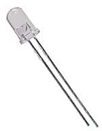
2 high intensity white LEDS (you can use other colors if desired)
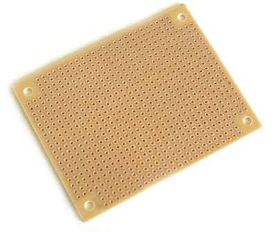
small perf board
2 470 ohm resistors
toggle switch or slide switch
9V battery snap
9V battery
small project box (you can use an Altoid tin)
electrical wire (about 2′ total)
soldering iron
solder
hot glue
electrical tape

For full assembly instructions, you can view the pages here:
http://www.instructables.com/id/9-Volt-Headlamp/

What causes oxidation on surface mount pads?

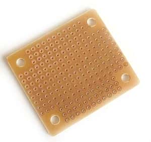
perf boardSolder contacts must meet minimum contact rating specifications to effectively be used. But sometimes you’ll begin to solder an electronic component to a board and realize that oxidation has occurred. Why does this happen?

Typically, there are two reasons that oxidation occurs on boards.

The main reason is improper storage and handling. Boards should be received from your supplier in a vacuum pack, which would render them clean and ready to accept solder. Once the vacuum seal has been broken, the boards are exposed to the environment. Boards that are stored in facilities with high humidity will experience accelerated deterioration. When handling boards, use only gloved hands and handle by the edges whenever possible.

Another way PCBs become contaminated is at the factory level. If your boards have just been removed from their packaging, chances are the problem is not oxidation. Much of the contamination is at the manufacturing level which is found after the bag has been opened. The main reasons this happens is because of incorrect ph levels, careless handling of the PCBs or if the boards are poorly washed with the surface film.

How can this be avoided? Handle the boards properly including using proper storage methods. Keep the boards in dry storage area, free from humidity. Make sure that anyone that handles them wears gloves to keep body oils from the pads and instruct everyone to touch only the edges of the boards. If your problems are from the factory, address the factory about the issues to avoid the same problems with future orders.

What Happens to Old Electronic Components and Boards?

We came across this blog post the other day and thought it was worth bringing here.

Here’s an excerpt:

Yesterday I had the opportunity to shoot video in a facility that is the largest company in America that recycles the glass from electronics and computers. The men who own this company, built the machines that separate and break up the glass, themselves.

Electronic products and computers are torn apart. The plastics are sold to one vendor while the electronics and circuit boards are sold to another. The glass fragments are then shipped to companies that melt it down and produce new glass.

I was impressed by how much of the material is able to find new life, rather than to be dumped into a landfill where it would simply sit for all time.

I hope that he’ll update his blog when this segment is aired – I’d love to see the whole process!