Category Archives: Diodes

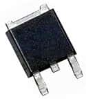
High-Voltage TVS Diodes as IGBT Active Clamp

Most high-voltage applications like power inverters, modern electric vehicles, and industrial control systems use IGBTs or Insulated Gate Bipolar Transistors, as they offer high-efficiency switching. However, as power densities are constantly on the rise in today’s electronics, the systems are subjected to greater demands. This necessitates newer methods of control. Littelfuse has developed new TVS diodes as an excellent choice to protect circuits against overvoltages when IGBTs turn off.

Most electronic modules and converter circuits contain parasitic inductances that are practically impossible to eliminate. Moreover, it is not possible to ignore their influence on the system’s behavior. While commuting, the current changes as the IGBT turns off. This produces a high voltage overshoot at its collector terminal.

The turn-off gate resistance of the IGBT, in principle, affects the speed of commutation and the turn-off voltage. Engineers typically use this technique for lower power level handling. However, they must match the turn-off gate resistance for overload conditions, short circuits, and for a temporary increase in the link circuit voltage. In regular operation, the generation of the overshoot voltage typically increases the switching losses and turn-off delays in the IGBTs, reducing the usability and or efficiency of the module. Therefore, high-power modules cannot use this simple technique.

The above problem has led to the development of a two-stage turn-off, with slow turn-off and soft-switch-off driver circuits, which operate with a gate resistance that can be reversed. In regular operations, the IGBT is turned off with the help of a gate resistor of low ohmic value, as this minimizes the switching losses. For handing surge currents or short circuits, this is changed to a high ohmic gate resistor. However, this also means that normal and fault conditions must be detected reliably.

Traditionally, the practice is to use an active clamp diode to protect the semiconductor during the event of a transient overload. The high voltage causes a current flow through the diode until the voltage transient dissipates. This also means the clamping diode is never subjected to recurrent pulses during operation. The IGBT and its driver power limit the problem of repetitive operation, both absorbing the excess energy. The use of an active clamp means the collector potential is directly fed back to the gate of the IGBT vial an element with an avalanche characteristic.

The clamping element forms the feedback branch. Typically, this is made up of a series of TVS or Transient Voltage Suppression diodes. When the collector-emitter voltage of the IGBT exceeds the approximate breakdown voltage of the clamping diode, it causes a current flow via the feedback to the gate of the IGBT. This raises the potential of the IGBT, reducing the rate of change of current at the collector, and stabilizing the condition. The design of the clamping diode then determines the voltage across the IGBT.

As the IGBT operates in the active range of its output characteristics, the energy stored in the stray inductance of the IGBT is converted to heat. The clamping process goes on until the stray inductance is demagnetized. Therefore, several low-voltage TVS diodes in series or a single TVS diode rated for high voltage are capable of providing the active clamping solution.

What is Diode Biasing?

PCB assemblies often contain numerous components. The engineer designing the board selects these components individually, based on their function in the circuit. For a successful project, it is essential to understand the basic operation of these components individually, and in relation to one another. One such component is the diode.

A diode is a semiconductor device with a PN junction. It supports current flow in only the forward direction—from the anode to the cathode—and not in the reverse. However, to allow current flow in the forward direction, a diode must be given a particular voltage to overcome the bias in its PN junction. Diode biasing is the application of a DC voltage across the diode’s terminals for overcoming the PN junction bias.

It is possible to bias a diode in two ways—forward and reverse. When forward biased, the diode allows current flow from its anode to its cathode, provided the biasing voltage is greater than the PN junction bias. However, when reverse-biased, the biasing voltage cannot overcome the PN junction bias, and the diode blocks any current flow. Reverse biasing a diode is a convenient way for using it to convert alternating current to direct current. Proper use of forward and reverse biasing also allows other functions, such as electronic signal control.

Diodes are mostly germanium or silicon-based. A diode consists of a layer of P-type semiconductor material and another layer of an N-type semiconductor material joined together. The P-type material forms the anode terminal and the N-type material forms the cathode terminal of the diode.

When fabricating a diode, the manufacturer dopes the two layers differently. They dope one of the layers with boron or aluminum to make it P-type, which gives it a slightly positive charge. The P-type semiconductor, therefore, has a deficit of electrons or an abundance of holes. They dope the other layer with phosphorus or arsenic to give it a slightly negative charge and make it N-type. Therefore, the N-type semiconductor has an abundance of electrons.

At the junction of the P-type and N-type layers, electrons and holes combine to form a sort of neutral zone. Therefore, when a current must flow, a voltage bias is necessary to push the electrons and holes through this neutral zone. The neutral zone is less than a millimeter in thickness.

A forward bias pushes holes from the P-type layer, across the neutral zone, into the N-type layer. The forward bias reduces the width of the neutral zone to allow the current to flow. The forward bias necessary depends on the material of the diode. It is 0.7 VDC for silicon diodes and about 0.3 VDC for germanium diodes.

On the other hand, a reverse bias adds more electrons to the N-type layer and holes to the P-type layer. This increases the width of the neutral zone, making it impossible for current to flow across it.

Therefore, forward biasing allows current flow through the diode from the anode to the cathode, and reverse biasing prevents current flow. Even with forward biasing, there is no current flow until the voltage is able to overcome the PN junction bias.

What are Diode Array Detectors?

High Performance Liquid Chromatography or HPLC uses diode arrays for recording the absorption spectrum of samples when ultraviolet and visible light passes through them. This enables the user to gather qualitative information about the samples. Major applications of HPLC diode array detectors include agriculture, environment, and industries such as petrochemical, energy, chemistry, life sciences, and pharmaceuticals.

Diode array detectors of HPLC have the advantage of the ability to select the best wavelength for analysis. Therefore, when selecting a diode array for use as a detector in HPLC, one should consider features such as resolution, wavelength range, near infrared ranges, baseline stability, low noise, and peak integration. Some vendors also offer the technique of detecting using a configurable light path formed from fiber optics.

An HPLC has a tungsten lamp emitting light in the visible range. This light enters a deuterium lamp that adds the UV to the visible light, forming a polychromatic beam. As this beam passes through a flow-cell, the sample in the flow-cell absorbs certain wavelengths. The output light then enters a grating, which splits the polychromatic beam into its constituent wavelengths and these pass through a slit before falling on an array of photodiodes, which measure their intensities.

As the diode array detectors measure all wavelengths simultaneously, it is able to acquire the spectra as well as the multiple single wavelengths at the same time by the different diodes in the array. The diode array detector has high selectivity, as it can identify different substances by their spectra.

One of the major advantages of the diode array detector is the tungsten lamp offering light in the extended visible wavelength. Additionally, by controlling the temperature of the optical unit of the diode array detector, its signal quality improves dramatically. Moreover, the diode array detector does not require a reference diode.

While other types of detectors use a diode for reference, for a diode array detector, there is no direct measurement of a signal when there is no absorption. Rather, the HPLC uses a detector balance. This happens automatically as the user switches the instrument on or just before conducting a measurement. The user achieves a detector balance by setting the absorption values for all wavelengths to zero. According to the Lambert Beer’s law, this allows the measurement of all intensities during an experiment to be made relative to this zero absorption intensity.

To cater to baseline changes or drift during a measurement, the diode array detector uses a reference wavelength. The user has to select a specific wavelength as reference, and make sure there is no absorption in the wavelength during the entire chromatography measurement. The user then uses the relative changes of the reference intensities for correcting the proportional changes occurring in other wavelengths.

Five factors majorly affect the measurements done by HPLCs using diode array detectors. These are the slit width, the bandwidth, the response time, and the flow cells. The user has to adjust all of them to obtain the best response from the diode array detector when testing the absorption of a sample. For instance, the slit defines the amount of light the detector measures. The bandwidth defines the window for the data acquisition. The response time defines the time resolution, and the flow cell defines the flow range.

Why Does An Inductor Need A Fly-Back Diode?

An inductor usually stores energy when current flows through it, and releases it once the current flow stops. When the power supply to an inductor is suddenly reduced or removed, the inductor generates a voltage spike, which is also referred to as an inductive fly-back. Any current flowing through the inductor cannot change instantly and is limited by the time constant of the inductor. This is similar to the time constant of a capacitor, which limits the rate of change of voltage across its terminals.

The time constant of an inductor is the product of its inductance in Henries and the resistance present in the circuit. Usually, all current can be considered to have been dissipated within five time constants once the inductor has been disconnected. The process of inductive fly-back is best explained with an example – a 10H inductor in series with a 10Ω resistor, is charged long enough through a closed switch so that maximum amount of current is now flowing through the circuit.
When the switch is suddenly opened, the current flow has to come to zero within five seconds (five time constants). However, the switch opens far faster than five seconds, which implies current flow through an open switch – an impossible situation.

However, this can be explained by considering the switch to be bridged by air resistance of an extremely high value – 40,000,000 MΩ. Therefore, the inductor, in trying to keep the current flowing through the circuit will send a minute amount of current through this big air-resistor. According to Ohm’s law, every resistor will have a voltage drop commensurate with the current flowing through it. To maintain the current flow in the same direction, the inductor will have to change the polarity of the voltage across itself.

At the instant the switch opened, the current through the circuit would have been about 99% of the maximum current. Such a current multiplied by the extremely high resistance of the air gap will result in a huge voltage. Such a large voltage drop is possible because the inductor has stored energy, which it will use to create a very large negative potential on one side of the gap. That ensures the current flow will match the dissipation curve of the inductor. This is the origin of the huge fly-back voltage spike associated with the sudden disruption of current through an inductor.

The fly-back voltage generated by an inductor can be potentially damaging. Not only can the arc generated damage the insulation of the inductor, it can damage the switch or component being used to open or close the circuit. The arcing effect has been dramatically captured in this short video.
The use of a fly-back diode precludes the possibility of damage from an inductive fly-back. The diode provides a path for the inductor to drive the current flow once the circuit has been opened. As long as the circuit is closed, the diode is reverse biased and does not contribute to the functioning of the circuit.

When the switch opens, the inductor has a path to maintain the current flow through the diode. As the inductor reverses its polarity, it forward biases the diode, which then conducts current for the five time constants, until the current reduces to zero. That prevents the voltage spike.

What are Zener, Schottky and Avalanche Diodes?

Diodes are very commonly used semiconductor devices. They are mostly used as rectifiers for converting Alternating to Direct current. Their special characteristic of allowing current flow in only one direction makes them indispensable as rectifiers. Apart from rectification, various types of diodes are available for different purposes such as for generating light, microwaves, infrared rays and for various types of switching at high speeds.

For example, the power supply industry has been moving towards high speed switching because higher speed reduces the volume of magnetics used, which ultimately reduces the bulk and price of the units. For switching at high frequencies, diodes are also required to react at high speeds. Schottky diodes are ideal for this purpose, as their switching speeds approach nearly zero time. Additionally, they have very low forward voltage drop, which increases their operating efficiency.

As their switching speed is very high, Schottky diodes recover very fast when the current reverses, resulting in only a very small reverse current overshoot. Although the maximum average rectified currents for Schottky diodes are popularly in the range of 1, 2, 3 and 10 Amperes, Schottky diodes that can handle up to 400A are also available. The corresponding maximum reverse voltage for Schottky diodes can range from 8 to 1200V, with most popular values being 30, 40, 60 and 100 Volts.

Another very versatile type of diode used in the power supply industry is the Zener diode. All diodes conduct current only when they are forward biased. When they are reverse biased, there is only a very small leakage current flowing. As the reverse voltage increases to beyond the rated peak inverse voltage of the diode, the diode can breakdown irreversibly and with permanent damage.

A special type of diode, called the Zener diode, blocks the current through it up to a certain voltage when reverse biased. Beyond this reverse breakdown voltage, it allows the current to flow even when biased in the reverse. That makes this type of diode very useful for generating reference voltages, clamping signals to specific voltage levels or ranges and more generally acting as a voltage regulator.

Zener diodes are manufactured to have their reverse breakdown voltage occur at specific, well-defined voltage levels. They are also able to operate continuously in the breakdown mode, without damage. Commonly, Zener diodes are available with breakdown voltage between 1.8 to 200 Volts.

Another special type of diode called the Avalanche diode is used for circuit protection. When the reverse bias voltage starts to increase, the diode intentionally starts an avalanche effect at a predetermined voltage. This causes the diode to start conducting current without damaging itself, and diverts the excessive power away from the circuit to its ground.

Designers use the Avalanche diode more as a protection to circuits against unwanted or unexpected voltages that might otherwise have caused extensive damage. Usually, the cathode of the diode connects to the circuit while its anode is connected to the ground. Therefore, the Avalanche diode bypasses any threatening voltage directly to the ground, thus saving the circuit. In this configuration, Avalanche diodes act as clamping diodes fixing the maximum voltage that the circuit will experience.

How did the diode get it’s name?

Although most diodes are made of silicon nowadays, it was not always so. Initially, there were two types – thermionic or vacuum tube and solid state or semiconductor. Both the types were developed simultaneously, but separately, in the early 1900s. Early semiconductor diodes were not as capable as their vacuum tube counterparts, which were extensively used as radio receiver detectors. Various types of these thermionic valves were in use and had different functionalities such as double-diode triodes, amplifiers, vacuum tube rectifiers and gas-filled rectifiers.

The diode gets its name from the two electrodes it has. Both the thermionic as well as the semiconductor type possess the peculiar asymmetric property of conductance, whereby a diode offers low resistance to flow of current in one direction and high resistance in the other. Similar to its vacuum counterpart, several types of semiconductor diodes exist.

The first semiconductor diode was the cat’s whisker type, made of mineral crystals such as galena and developed around 1906. However, these were not very stable and did not find much use at the time. Different materials such as selenium and germanium are also used for making these devices.

In 1873, Frederick Guthrie discovered that current flow was possible only in one direction and that was the basic principle of the thermionic diodes. Guthrie found that it was possible to discharge a positively charged electroscope when a grounded piece of white-hot metal was brought close to it. This did not happen if the electroscope was negatively charged. This gave him proof that current can flow only in one direction.

Although Thomas Edison rediscovered the same principle in 1880 and took out a patent for his discovery, it did not find much use until 20 years later. In 1900s, John Ambrose Fleming used the Edison effect to make and patent the first thermionic diode, also called the Fleming valve. He used the device as a precision radio detector.

To put it simply, a diode functions as a one-way valve. It allows electricity to flow in one direction while blocking all current flow in the reverse direction. The semiconductor diode has an anode (A, p-type or positive) and a cathode (K, n-type or negative). Since the cathode is more negatively charged compared to the anode, electric current will not flow if the cathode and anode are charged to the same or very similar voltage.

This property of the diode allowing current to flow in only one direction is utilized during rectification, when alternating current is changed to direct current. Such rectifier diodes are mostly used in low current power supplies. For turning a circuit on or off, you need a switching diode. If you are working with high-frequency signals, band-switching diodes are useful. Where a constant voltage is necessary, there are zener diodes.

Diodes are also used for various purposes such as the production of different types of analog signals, microwave frequencies and even light of various colors. When current passes through Light Emitting Diodes or LEDs, it emits light of a specific wavelength. Such diodes are used for displays, room lighting and for decoration.

Turn your old PC fans into mini wind generators

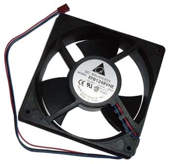
pc fanHere’s a great project that you can do either to experiment with wind turbines or to generate some energy! While the amount of energy produced is not overwhelming, this project can sure get your brain moving in the right direction.

The best thing about this project is that you probably already have everything you need lying around:

  • Thick plastic bottle
  • Old PC fan, bigger the better!
  • A few feet of small wire
  • A piece of wood about 1.5″ square and around 20cm long
  • Two lengths of steel tubing that slide inside of each other, about 1/2″
  • 6 Schottkey diodes
  • Epoxy
  • Super Glue
  • Zip ties
  • An old CD

You can find the full instructions including video here: http://www.instructables.com/id/Upcycle-your-old-PC-fans-into-mini-wind-generators/

If you want to have a kid-friendly wind turbine kit that already has all the pieces you need, we sell one of those. Our kits come with full instructions and all the materials needed to try your hand at creating a source of renewable energy – a wind turbine. The kit also comes with different experiments you can try with your wind turbine once it’s assembled. Great project for summer for the kids!

West Florida Components is Social!

Are you doing the whole Facebook thing? How about Twitter?

Well, we are….and we’re also on StumbleUpon, Digg, Delicious and a whole bunch more.

Why should you care? Because we give away a lot of discounts to our Facebook Fans and Twitter Followers! And our Facebook Fans and Twitter Followers are the first to know about newly discounted electronic components, parts and supplies.

We never overload our customers with too much communication but we like to keep in touch. The social media sites have given us a wonderful platform to connect with our customers.

Facebook

Facebook

So the next time your on Facebook, don’t forget to add our Fan Page to your list….we’re the same name over there as we are here: WestFloridaComponents (no spaces):
West Florida Components on Facebook

And here’s our Twitter user ID: westfloridacomp (had to be shortened because of their site):
West Florida Components on Twitter

So next time you feel like socializing, come on over and introduce yourself! We’d be thrilled to meet you.

The Titan – Newest (and biggest) Vacuum Tube Amp from Steve

Just in from our friend Steve W. in Canada (who constructs the most amazing vacuum tube amplifiers)…

The best way to describe this next amplifier is it’s a Titan. It has to be the biggest, baddest, heaviest and most powerful amplifier I’ve made to date! Weighing in at just under 60 lbs. this push-pull-parallel EL-34 / 6L6 is conservatively rated at 110 watts per channel using EL-34 tubes. Capable of driving 4 or 8 ohm speakers via a switch on the back panel, this amp is a tube roller’s dream.

Simply by plugging in which rectifier tubes you want to use, be it a pair of 5Y3’s, 5R4’s, 5U4’s or even 5AR4’s you can match the correct plate voltage with what ever power tubes you choose, be it a set of 6V6’s, 6L6’s, 5881’s Kt-66’s, Kt-77’s, EL-34’s, or even 7591’s.

You also have the choice of running the amp in push-pull instead of push-pull-parallel simply by not installing the front four power tubes and switching off one of the two rectifier tubes via a switch located on the right hand side of the chassis. The signal and phase-inverter pre amp tubes used are my favourite large dual triodes 6SN7’s.

Now, about the transformers, seeing that this amplifier has to drive thirteen tubes, I thought it only made sense to use a separate filament power transformer. The transformer right next to the larger power transformer is the 20 amp filament transformer. By doing this, I’ve removed the heater load off of the main power transformer which now only has to supply the high voltages the amp needs.

Along with a hefty octet of 470 mfd 400 volt capacitors bought from West Florida Components, there is more than enough capacitance to keep this amp in the black during those high current moments when the music demands it.

By sharing the load this way, the main power transformer will not be taxed nearly as much. The output transformers are massive Hammonds that can easily handle the wattage this amp delivers.

You will notice a volume control knob located right smack in the middle of the mirror in front of the amp that’s surrounded in pure copper foil, and that is because this is a fully integrated power amp with a line stage pre amplifier built into it. That means you do not need to buy a separate pre amplifier. You only need to plug in your CD player, satellite, MP3, I-pod, or what ever type of line stage device you like to use, directly into the amplifier.

There are two benefits to an integrated amp, one, you don’t have to go out and spend money on a separate pre amp, and two, you are amplifying completely with tubes throughout the whole amplifying process from pre amp to power amp, and that makes it sound better, way better!

Once again – amazing job, Steve! Thanks for sharing this with our readers.

Schottky Diodes – What makes them so special?

Some of the most common questions we get are about Schottky diodes.

Schottky Diode

The simple definition of a Schottky diode is a diode with a very fast switching action as well as a lower forward voltage drop.

As the current flows through a diode, it experiences a slight voltage drop across the diode terminals. Normally, a diode has approximately 0.7-1.7V drops. A Schottky diode, however, will see a drop in voltage between 0.15-0.45V. The benefit of this lower drop? A much higher system efficiency.

The construction of a Schottky diode also effects the voltage drop and switching time. A Schottky diode has a metal semiconductor junction as the Schottky barrier rather than the traditional semiconductor to semiconductor junction seen in conventional diodes. It is this barrier that affects the voltage drop and the speed of the switching times.

Sometimes Schottky diodes are misspelled by adding an ‘e’ to the end: Schottkey. The correct spelling is Schottky which is the surname of the man that is credited with putting these electronic components in the history books.